Products
Categories
New products
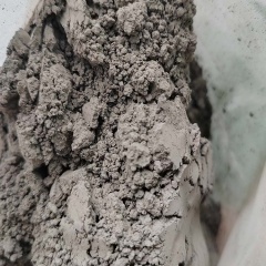
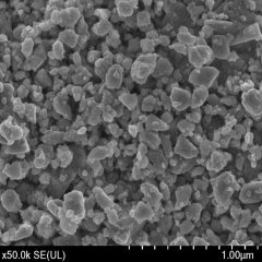
99.99% high purity beta sic nano powders Our 4N nano β-SiC (99.99% purity) is precision-synthesized via CVD, delivering ultra-fine particle size with exceptional sintering activity for high-density ceramic components. It thrives in the most demanding semiconductor environments — from CMP chucks and lithography stages to plasma etch focus rings and chamber liners. Its chemical inertness and minimal metal impurity outgassing maximize chip yield where it matters most. Trusted by leading fabs and equipment makers worldwide. more
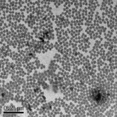
Monodisperse spherical Nano SiO₂ aqueous dispersion/colloid This transparent SiO₂ aqueous dispersion is synthesized via patented sol-gel technology, featuring optical excellence visible light transmittance and shelf life >18 months under ambient storage. It is widely used in electronics as low-k dielectric materials, in biomedicine as drug carriers, and in optics for anti-reflection coatings. more
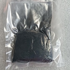
Magnéli Phase Nano Titanium suboxide Ti₄O₇ Powder Magnéli phase Nano titanium suboxide (Ti₄O₇) is an advanced functional material with a unique crystal structure, appearing as a blue-black powder with a precisely controlled particle size of 200–300 nm and a purity of up to 99.9%. As an important member of the titanium oxide family, Ti₄O₇ combines excellent electrical conductivity, chemical stability, and catalytic activity, making it an ideal choice for new energy, environmental protection, and electronics applications. more
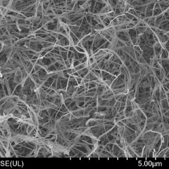
Boron Nitride Nanotubes(BNNTs): High Thermal Conductivity Heat Dissipation Fillers BNNTs share the tubular structure of carbon nanotubes but deliver fundamentally different properties: electrical insulation, superior thermal stability (up to 900°C in air), and high thermal conductivity. With a wide bandgap of ~5.5 eV, they offer consistent, predictable performance where CNTs fall short. more
Phase-Smart VO₂ Nanoparticles: Intelligent Thermal Response, Engineered to Order From Thermochromic Color Change material to Intelligent Temperature Control material: The Performance Revolution and Application Blueprint of Vanadium Dioxide and Tungsten-Doped VO2 more
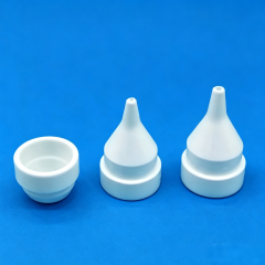
Precision Ceramic 3D Printing Solutions turns impossible structures into reality Precision Ceramic 3D Printing Solutions – Redefining the boundaries of ceramic manufacturing, from dental restorations to aerospace-grade high-temperature components.Precision ceramic 3D printing turns impossible structures into reality. more
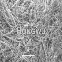
New conductive material nickel nanowires NiNWs Hongwu Nickel nanowires have a wide range of potential applications in electronic materials, catalysis, polymers, magnetic storage ultra-high density recording materials, sensors and self-lubricating materials. more
Transparent Colloidal Ag Antibacterial Nano Silver Colloid Ag (Antibacterial Nano Silver Colloid) has been well known antibacterial, antiviral and antifungal properties are enhanced by small particle size and large surface area. more
Nano silica particles used in epoxy resin, superhydrophobic coating nano silica powder Nano silica particles, 20-30nm, 99.8% purity, widely used in exposy resin and superhydrophobic coating. more
Latest news
Some nanomaterials for Thermochromic Application
Thermochromism refers to the phenomenon where a material undergoes color changes under temperature changes. This change is usually caused by changes in the electronic or molecular structure of the material. Its application principle mainly involves t...
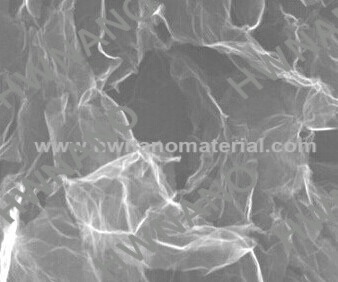
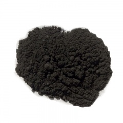
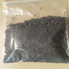
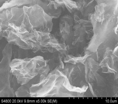
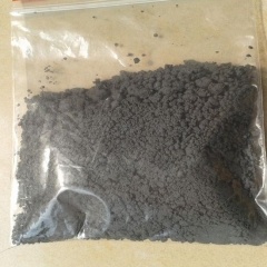
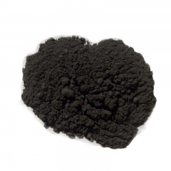
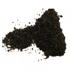
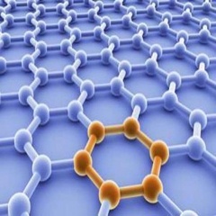
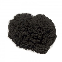
Graphene nanopowders has single layer and multi layer, widely used in solar cells.
product origin:
Chinaitem no.:
C952shipping port:
Guangzhoucolor:
black powderlead time:
3payment:
T/T, PayPalSingle Layer Graphene Nanopowders Used as Solar Cells
Spec: thickness:0.6-1.2nm,Length:0.8-2um,>99%
Application for Single layer graphene nanopowders:
1. Nanoelectronic devices: graphene at room temperature with 10 times the high carrier mobility of commercial wafers (about10 am / V • s), and is affected by temperature and doping effect is very small,showing room temperature ballistic transport properties of sub-micron scale,which is graphene nanoelectronic devices as the most prominent advantages of the electronic engineering attractive room ballistic FET possible nano scale graphene reduced to the same or even a single benzene ring maintaining good stabilityand electrical properties, making it possible to explore single-electrondevices.
2. Instead of silicon production super computer:Graphene is the best known properties of the conductive material, the particular characteristics of graphene for high-frequency circuits. Since the emergence of graphene, the development prospects of high frequency boost seemsto become infinitely wide, which makes it in the microelectronics field alsohas great potential. They even graphene as a substitute for silicon, can beused to produce future supercomputers.
3. Photon sensor: Graphene for photon sensor,such a sensor for detecting information carried in the optical fiber. Graphene also be used for solar cells and liquid crystal display, because the grapheneis transparent, use it to manufacture panels having more excellent than theother light-transmissive material.
4. Gene sequencing: The thickness of theconductive graphene DNA chain is smaller than the adjacent electron fingerprintexists between the distance between the base and the four DNA bases, therefore,expected to achieve graphene direct, rapid, low cost of gene sequencingtechnology electronics.
5. Other applications: Graphene transistors canalso be applied, touch screen can also be used to make bandages, food packagingand even antimicrobial T unmoving, with graphene do photoelectrochemical cellcan replace metal-based organic light-emitting diode, because graphene You canalso replace the traditional lamp metal graphite electrodes make it easier to recycle.Substances can be used to develop not only produce paper-thin ultra-lightaircraft materials, manufacturing surplus tough armor.
6. Graphene can also do a soft transparent electrode, ultrafast optical sensing device excellent raw materials, can be usedin manufacturing solar panels. Graphene research into optical modems, isexpected to improve the speed 10,000 times.
Previous :
Transparent Conductive Electrode Multi Layer Graphene NanopowdersNext :
Conductive Multi-layer Graphene Nano PowdersEmail us with any questions or inquiries or use our contact data. We would be happy to answer your questions.
Copyright © 2010-2026 Hongwu International Group Ltd All Rights Reserved.
The professional team to service !
8620-87226359,8620-87748917
hwnano@xuzhounano.com
hwnano